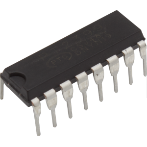
Integrated Circuit - AS3340A, VCO, Alfa, 16-Pin Dip
The AS3340A is Alfa’s version of the CEM3340 IC. The AS3340A is a completely self-contained, precision voltage controlled oscillator, featuring both exponential and linear control scales and up to four buffered output waveforms: triangle, sawtooth, square, and pulse with voltage controllable pulse width. Full temperature compensation makes these VCOs extremely stable, and eliminates the need for a temperature compensation resistor. The highly accurate exponential and linear control inputs are virtual ground summing nodes, allowing multiple control voltages to be mixed within the device itself.
Also included is provision for hard and soft synchronization of the frequency, and an output for easy adjustment of high frequency tracking. Special care in the design ensures oscillation start-up under any power-on sequence and supply conditions.
An on-chip 7.4 volt Zener diode allows the device to operate off ±15 volt supplies, as well as +12, -5 volt supplies. For voltages greater than -7.5 volts, a series current limiting resistor REE must be added between pin 3 and the negative supply. Its value is calculated as follows:
REE = (VEE - 7.4) / .008
To minimize self-heating and improve thermal-stability it is recommended to keep VEE = -5V (external power supply).
External VEE also minimizes current through GND and improves VCO stability. Scale1 and Scale2 pins are used for trimming of thermo-compensation circuit. Resistor RZ, connected to Scale 1 pin, should provide the same current as current (approx.. 100 uA) flowing in Scale2 pin determined by resistor RT = 5.72k. Rs , resistor connected to pin Scale, is intended to trim V/oct range. AS3340A is an improved version of AS3340. AS3340A has much more output frequency stability against Vcc and VEE . Frequency stability can be improved If external reference voltage (with level approximately ⅓ Vcc) is connected to pin 9 (Soft Sync. Input). AS3340A benefits from improved symmetry of rising and falling edge of triangle signal (approx.. 50%).
The AS3340A is available in a 16-pin DIP package.
Features
- Large Sweep Range: 500,000:1
- Fully Temperature Compensated
- Four Output Waveforms Available; No waveform trimming required
- Summing Node Inputs for Frequency Control
- High Exponential Scale Accuracy
- Low Temperature Drift
- Voltage Controlled Pulse Width
- Hard and Soft Sync Inputs
- Linear FM
- Buffered, Short Circuit Protected Outputs
- ±15 Volt Supplies
| Exponential Scale Error, Trimmed | 0.05% | ||
| Exponential Scale Error, Untrimmed | 0.2% | ||
| Frequency Control Range | 500K:1 | ||
| Hard Sync Input Resistance | 6.3 KΩ | ||
| Hard Sync Reference Voltage | -1.4 V | ||
| Input Bias Current at Reference and Control Current Inputs | 200 nA | ||
| Max. Current through Any Pin | ±40 mA | ||
| Max. Operating Temperature Range | - 25°C to 75°C | ||
| Max. Storage Temperature Range | - 55°C to 120°C | ||
| Max. Voltage Between Frequency Control Pin or Reference Current Pin and GND Pin | ±6 V | ||
| Max. Voltage Between Multiplier Output Pin and GND Pin | +6 V, -1 V | ||
| Max. Voltage Between VCC and GND Pins | +18 V, -0,5 V | ||
| Max. Voltage Between VCC and VEE Pins | +24 V, -0,5 V | ||
| Max. Voltage Between VEE and GND Pins | -6 V, +0,5 V | ||
| Max Capacitor Charge/Discharge Current | 570 µA | ||
| Multiplier Gain Errors | 0.0005%/µA | ||
| Negative Supply Voltage Range (Current limiting resistor required for negative supplies greater than -6 volts) | -4.5V to -18V | ||
| Offset Voltage at Reference and Control Current Inputs | 0 mV | ||
| Oscillator Drift | ±50 ppm | ||
| PWM Input Pin Current | 1.5 µA | ||
| PWM Input Voltage for 0% Pulse Width | 0 mV | ||
| PWM Input Voltage for 100% Pulse Width | 5 V | ||
| Positive Supply Current | 5 mA | ||
| Positive Supply Voltage Range | +10V to +18V | ||
| Pulse Output Source Capability at +10V | 10 mA | ||
| Sawtooth Output Sink Capability | 800 µA | ||
| Sawtooth Waveform Lower Level | 0 mV | ||
| Sawtooth Waveform Upper Level | 10.0 V | ||
| Squarewave Output Levels | -1.3 V | ||
| Tempco of Input Bias Currents | 0 ppm | ||
| Tempo Cancellation | 0 ppm | ||
| Triangle & Sawtooth Output Impedance | 100 Ω | ||
| Triangle Buffer Input Current | 0.3 nA | ||
| Triangle Output Sink Capability | 550 µA | ||
| Triangle Waveform Lower Level | 0 mV | ||
| Triangle Waveform Symmetry | 50% | ||
| Triangle Waveform Upper Level | 5.0 V | ||
| Packaging Dimensions | 0.72 in. × 0.36 in. × 0.283 in. | ||
| Weight (Packaging) | 0.0033 lbs. | ||
| All Models |
My Project Lists
Specifications, Files, and Documents
Customers who purchased this item also bought


Product Reviews